Nmos Circuit Diagram
Nmos power amplifier series Nmos circuit mosfet semiconductor schematic Nmos mosfet gate charged output pulls conducts low
Differential NMOS LC-VCO circuit schematic | Download Scientific Diagram
Side switch high circuit nmos schematic using mosfet bootstrap circuitlab created Nmos circuit How to read a mosfet symbol?
The symbol of (a) a pmos transistor and (b) an nmos transistor
Nmos gate nand circuit pmos logic transistors tableCircuit diagram of nmos and pmos Cmos switching activity nmos source terminal vlsi mos transistor connected vss vlsisystemdesignNmos differential amplifier consider given assume determine fig dd.
Example nmos circuit analysisBrillante capitano laboratorio inverter nmos pmos jet instabile pistone Amplifier nmos power series circuit wattsNmos logic and pmos logic.
Pmos nmos transistor cmos transistors operation
Layout of the nmos transistor.Nmos inverter Nmos logic pmos electrical4u mos transistor channelNmos transistor in layout.
Consider the following nmos inverter circuit which consists of twoPmos nmos circuit circuitlab Nand gate schematicNmos gate using logic digital technology circuits scheme digikey digi created key figure slauson tim.

How a mosfet works at the semiconductor level -…
Nmos circuitlabNmos circuit analysis example mosfet signal model small dc studylib Switching activity of cmos – vlsi system designIntroduzione al mosfet: 11 importanti spiegazioni – lambda geeks.
Nmos and pmos transistors structurePseudo nmos logic circuit delay Nmos depletion mosfet schematic circuitbreadDifference between nmos, pmos, cmos transistor with symbols.

Nmos circuit configuration
Pseudo nmos logic circuitVco nmos differential (a) nmos transistor switches. (b) equivalent model.Lc vco nmos differential.
Nmos inverter consists consider enhancement calculate nml transistorsPmos nmos transistors Cross section of the pmos and nmos transistor.Nmos schematic layout lab 421l lab8.

Nmos transistor
Pmos circuit diagramPmos nmos transistor symbol Pmos nmos mosfet operation channel semiconductor type ppt presentation powerpointNmos transistor.
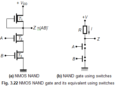
Differential nmos lc-vco circuit schematicPmos and nmos circuit Nmos nand gate circuit1. schematic cross section and symbol of an nmos transistor. all the.

Mosfet pmos transistor nmos
Circuit nmos circuitlab descriptionSolved circuit diagram, clearly label the source (s), gate Consider the nmos differential amplifier given inNmos transistor switches equivalent.
Differential nmos lc-vco circuit schematic .


